S29JL064J55TFI000
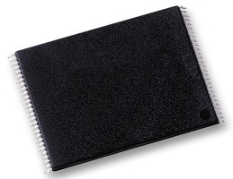
闪存, 并行NOR, 64 Mbit, 8M x 8bit / 4M x 16bit, CFI, 并行, TSOP, 48 引脚

需要更多?
| 数量 | 价钱 (含税) |
|---|---|
| 1+ | CNY74.200 (CNY83.846) |
| 10+ | CNY68.840 (CNY77.7892) |
| 25+ | CNY66.920 (CNY75.6196) |
| 50+ | CNY64.130 (CNY72.4669) |
| 100+ | CNY62.520 (CNY70.6476) |
| 250+ | CNY61.650 (CNY69.6645) |
| 500+ | CNY55.660 (CNY62.8958) |
S29JL064J55TFI000 的替代之选
找到 2 件产品
产品概述
The S29JL064J55TFI000 is a 64MB CMOS simultaneous Read/Write Flash Memory organized as 4194304 words of 16-bit each or 8388608 bytes of 8-bit each. Word mode data appears on DQ15-DQ0, byte mode data appears on DQ7-DQ0. The device is designed to be programmed in-system with the standard 3VCC supply and can also be programmed in standard EPROM programmers. The device is available with an access time of 55ns. Standard control pins - chip enable (CE#), write enable (WE#) and output enable (OE#) - control normal read and write operations and avoid bus contention issues. The device requires only a single 3V power supply for both read and write functions. Internally generated and regulated voltages are provided for the program and erase operations.
- Standard configuration
- Data can be continuously read from one bank while executing erase/program functions in another bank
- Zero latency between read and write operations
- Flexible bank architecture
- Read may occur in any of the three banks not being programmed or erased
- Four banks may be grouped by customer to achieve desired bank divisions
- Top and bottom boot sectors in the same device
- Any combination of sectors can be erased
- Manufactured on 0.11µm process technology
- Secured silicon region - Extra 256-byte sector
- Sophisticated power management circuits reduce power consumed during inactive periods to nearly zero
- Compatible with JEDEC standards
- Pinout and software compatible with single-power-supply flash standard
- High performance
- Program time - 7µs/word typical using accelerated programming function
- Ultralow power consumption
- Cycling endurance - 1million cycles per sector typical
- Data retention - 20 years typical
- Supports common flash memory interface
- Erase suspend/erase resume
技术规格
并行NOR
8M x 8bit / 4M x 16bit
TSOP
-
2.7V
-
-40°C
3V Parallel NOR Flash Memories
No SVHC (25-Jun-2025)
64Mbit
CFI, 并行
48引脚
55ns
3.6V
表面安装
85°C
MSL 3 - 168小时
法律与环境
进行最后一道重要生产流程所在的地区原产地:Thailand
进行最后一道重要生产流程所在的地区
RoHS
RoHS
产品合规证书