Print Page
BUK6D30-40EX
Power MOSFET, Trench, N Channel, 40 V, 18 A, 0.023 ohm, DFN2020MD, Surface Mount

Image is for illustrative purposes only. Please refer to product description.
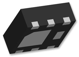
ManufacturerNEXPERIA
Manufacturer Part NoBUK6D30-40EXCopy
Manufacturer Standard Lead Time32 weeks
Order Code
Re-Reel3438511RL
Cut Tape3438511
Your Part Number
4,344 In Stock
6,000 more incoming. You can reserve stock now
4,344 Delivery in 5-6 Business Days(UK stock)
Packaging Options
| Packaging Type | Quantity | Unit Price: | Total |
|---|---|---|---|
| Cut Tape | 5 | CNY5.740 | CNY28.70 |
Cut Tape & Re-Reel
| Quantity | Price (inc GST) |
|---|---|
| 5+ | CNY5.740 (CNY6.4862) |
| 10+ | CNY3.550 (CNY4.0115) |
| 100+ | CNY2.280 (CNY2.5764) |
| 500+ | CNY1.740 (CNY1.9662) |
| 1000+ | CNY1.570 (CNY1.7741) |
| 5000+ | CNY1.320 (CNY1.4916) |
Line Note
Added to your Order Confirmation, Invoice, and Dispatch note for this order only.
Product Information
ManufacturerNEXPERIA
Manufacturer Part NoBUK6D30-40EXCopy
Manufacturer Standard Lead Time32 weeks
Order Code
Re-Reel3438511RL
Cut Tape3438511
Technical Datasheet
Channel TypeN Channel
Drain Source Voltage Vds40V
Continuous Drain Current Id18A
Drain Source On State Resistance0.023ohm
Transistor Case StyleDFN2020MD
Transistor MountingSurface Mount
Rds(on) Test Voltage10V
Gate Source Threshold Voltage Max1.6V
Power Dissipation19W
No. of Pins6Pins
Operating Temperature Max175°C
Product Range-
QualificationAEC-Q101
SVHCNo SVHC (25-Jun-2025)
Product Overview
BUK6D30-40EX is a 40V, N-channel Trench MOSFET. It is an N-channel enhancement mode Field-Effect Transistor (FET) in a medium power DFN2020MD-6 (SOT1220) Surface-Mounted Device (SMD) plastic package using Trench MOSFET technology. Typical applications include relay driver, high-speed line driver, low-side load switch, and switching circuits.
- Extended temperature range Tj = 175°C
- Side wettable flanks for optical solder inspection
- ElectroStatic Discharge (ESD) protection > 2kV HBM (class H2)
- AEC-Q101 qualified
- Drain-source breakdown voltage is 40V min at ID = 250µA; VGS = 0V; Tj= 25°C
- Gate-source threshold voltage is 1.6V typ at ID = 250µA; VDS = VGS; Tj = 25°C
- Drain-source on-state resistance is 23mohm typ at VGS = 10V; ID = 6A; Tj = 25°C
- Total gate charge is 8nC typ at VDS = 20V; ID = 5A; VGS = 10 V; Tj = 25°C
- Source-drain voltage is 0.8V typ at IS = 1.6A; VGS = 0V; Tj = 25°C
- Reverse recovery time is 11ns typ at IS = 1.6A; dIS/dt = -100A/µs; VGS = 0V; VDS = 20V; Tj = 25°C
Technical Specifications
Channel Type
N Channel
Continuous Drain Current Id
18A
Transistor Case Style
DFN2020MD
Rds(on) Test Voltage
10V
Power Dissipation
19W
Operating Temperature Max
175°C
Qualification
AEC-Q101
SVHC
No SVHC (25-Jun-2025)
Drain Source Voltage Vds
40V
Drain Source On State Resistance
0.023ohm
Transistor Mounting
Surface Mount
Gate Source Threshold Voltage Max
1.6V
No. of Pins
6Pins
Product Range
-
MSL
MSL 1 - Unlimited
Technical Docs (2)
Legislation and Environmental
Country of Origin:
Country in which last significant manufacturing process was carried outCountry of Origin:China
Country in which last significant manufacturing process was carried out
Country in which last significant manufacturing process was carried outCountry of Origin:China
Country in which last significant manufacturing process was carried out
Tariff No:85412900
US ECCN:EAR99
EU ECCN:NLR
RoHS Compliant:Yes
RoHS
RoHS Phthalates Compliant:Yes
RoHS
SVHC:No SVHC (25-Jun-2025)
Download Product Compliance Certificate
Product Compliance Certificate
Weight (kg):.004749