NX3DV2567HR,115
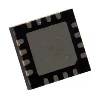
模拟开关, 1通道, 4PDT, HXQFN-16

需要更多?
| 包装类型 | 数量 | 单价 (不含增值税): | 合计 |
|---|---|---|---|
| 切割卷带 | 1 | CNY8.690 | CNY8.69 |
| 数量 | 价钱 (含税) |
|---|---|
| 1+ | CNY8.690 (CNY9.8197) |
| 10+ | CNY6.710 (CNY7.5823) |
| 50+ | CNY6.170 (CNY6.9721) |
| 100+ | CNY5.450 (CNY6.1585) |
| 250+ | CNY5.120 (CNY5.7856) |
| 500+ | CNY4.910 (CNY5.5483) |
| 1000+ | CNY4.760 (CNY5.3788) |
产品信息
产品概述
NX3DV2567HR,115 is a four-pole double-throw analogue switch (4PDT) optimized for switching WLAN-SIM supply, data and control signals. It has one digital select input (S) and four switches each with two independent input/outputs (nY0 and nY1) and a common input/output (nZ). Schmitt trigger action at S makes the circuit tolerant to slower input rise and fall times across the entire VCC range from 1.4V to 4.3V. A low input voltage threshold allows pin S to be driven by lower level logic signals without significant increase in supply current ICC. This makes it possible for the NX3DV2567 to switch 4.3V signals with a 1.8V digital controller, eliminating the need for logic level translation. The NX3DV2567 allows signals with amplitude up to VCC to be transmitted from nZ to nY0 or nY1; or from nY0 or nY1 to nZ. Applications include cell phone, PDA, digital camera, printer and notebook, LCD monitor, TV and set-top box.
- Very low ON resistance for supply path (0.5ohm (typ) at VCC = 1.8V, 0.45ohm (typical) at VCC = 2.7V)
- Low ON resistance for data path (7ohm (typical) at VCC = 1.8V, 6ohm (typical) at VCC = 2.7V)
- Low ON capacitance for data path
- Wide -3db bandwidth of <gt/>160MHz
- Break-before-make switching, high noise immunity
- ESD protection, CMOS low-power consumption
- Latch-up performance exceeds 100mA per JESD 78B Class II Level A
- 1.8V control logic at VCC = 3.6V Control input accepts voltages above supply voltage
- Very low supply current, even when input is below VC High current handling capability
- HXQFN16U package, -40°C to +125°C temperature range
技术规格
- 芯片功能
模拟开关
通态电阻最大值10.5ohm
IC 外壳 / 封装HXQFN
通道数1放大器
导通电阻最大值10.5ohm
多路复用器/解复用器配置-
芯片安装表面安装
工作温度最高值125°C
合规-
SVHC(高度关注物质)No SVHC (27-Jun-2024)
电源类型单电源
电源电压范围1.4V 至 4.3V
针脚数16引脚
导通电阻典型值6ohm
开关配置4PDT
接口-
工作温度最小值-40°C
产品范围-
湿气敏感性等级MSL 1 -无限制
法律与环境
- 原产地:
进行最后一道重要生产流程所在的地区原产地:Thailand
进行最后一道重要生产流程所在的地区税则号:85423990US ECCN:EAR99EU ECCN:NLRRoHS 合规:是RoHS
RoHS 邻苯二甲酸盐合规:是RoHS
SVHC:No SVHC (27-Jun-2024)下载产品合规证书产品合规证书
重量(千克):.0003