Print Page
5PB1104CMGK/W
Clock Buffer, 200MHz, 4 Outputs, 3.3V, DFN-8, -40°C to 105°C

Image is for illustrative purposes only. Please refer to product description.
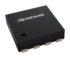


ManufacturerRENESAS
Manufacturer Part No5PB1104CMGK/WCopy
Order Code
Re-Reel4243569RL
Cut Tape4243569
Your Part Number
Available to Order
register your interest here
Packaging Options
| Packaging Type | Quantity | Unit Price: | Total |
|---|---|---|---|
| Cut Tape | 1 | CNY15.070 | CNY15.07 |
Cut Tape & Re-Reel
| Quantity | Price (inc GST) |
|---|---|
| 1+ | CNY15.070 (CNY17.0291) |
| 10+ | CNY13.570 (CNY15.3341) |
| 50+ | CNY12.760 (CNY14.4188) |
| 100+ | CNY11.860 (CNY13.4018) |
| 250+ | CNY11.050 (CNY12.4865) |
| 500+ | CNY10.650 (CNY12.0345) |
| 1000+ | CNY10.350 (CNY11.6955) |
| 2500+ | CNY10.140 (CNY11.4582) |
Line Note
Added to your Order Confirmation, Invoice, and Dispatch note for this order only.
Product Information
ManufacturerRENESAS
Manufacturer Part No5PB1104CMGK/WCopy
Order Code
Re-Reel4243569RL
Cut Tape4243569
Technical Datasheet
Clock IC TypeClock Buffer
Frequency200MHz
Clock IC Case StyleDFN
No. of Outputs4Outputs
Supply Voltage Min1.8V
Supply Voltage Max3.3V
IC Case / PackageDFN
No. of Pins8Pins
Product Range-
QualificationAEC-Q100
Operating Temperature Min-40°C
Operating Temperature Max105°C
Automotive Qualification StandardAEC-Q100
SVHCNo SVHC (25-Jun-2025)
Product Overview
5PB1104CMGK/W is a 5PB11xx series high-performance LVCMOS clock buffer. It has an additive phase jitter of 50fs RMS. There are five different fan-out variations available: 1:2 to 1:10. The 5PB11xx supports a synchronous glitch-free output enable (OE) function to eliminate any potential intermediate incorrect output clock cycles when enabling or disabling outputs. Typical applications include industrial applications automotive, radar, lidar, and other applications.
- High-performance 1:2, 1:4, 1:6, 1:8, 1:10 LVCMOS clock buffer
- Very low pin -to-pin skew: < 50ps
- Very low additive jitter: < 50fs
- Supply voltage range from 1.8V to 3.3V
- 3.3V tolerant input clock
- Maximum frequency of 200MHz
- Integrated serial termination for 50 ohm channel
- Available in 8 pin DFN package
- Temperature range from -40°C to +105°C
Technical Specifications
Clock IC Type
Clock Buffer
Clock IC Case Style
DFN
Supply Voltage Min
1.8V
IC Case / Package
DFN
Product Range
-
Operating Temperature Min
-40°C
Automotive Qualification Standard
AEC-Q100
Frequency
200MHz
No. of Outputs
4Outputs
Supply Voltage Max
3.3V
No. of Pins
8Pins
Qualification
AEC-Q100
Operating Temperature Max
105°C
SVHC
No SVHC (25-Jun-2025)
Technical Docs (2)
Legislation and Environmental
Country of Origin:
Country in which last significant manufacturing process was carried outCountry of Origin:Thailand
Country in which last significant manufacturing process was carried out
Country in which last significant manufacturing process was carried outCountry of Origin:Thailand
Country in which last significant manufacturing process was carried out
Tariff No:85423990
US ECCN:EAR99
EU ECCN:NLR
RoHS Compliant:Yes
RoHS
RoHS Phthalates Compliant:Yes
RoHS
SVHC:No SVHC (25-Jun-2025)
Download Product Compliance Certificate
Product Compliance Certificate
Weight (kg):.00001