Print Page
NVMFD5C446NLT1G
Dual MOSFET, N Channel, 40 V, 40 V, 145 A, 145 A, 0.00265 ohm

Image is for illustrative purposes only. Please refer to product description.
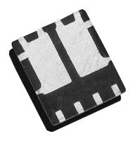
ManufacturerONSEMI
Manufacturer Part NoNVMFD5C446NLT1GCopy
Manufacturer Standard Lead Time27 weeks
Order Code
Re-Reel2835598RL
Cut Tape2835598
Your Part Number
1,410 In Stock
Need more?
10 Next business day delivery available(Shanghai stock)
1,400 Delivery in 5-6 Business Days(UK stock)
Packaging Options
| Packaging Type | Quantity | Unit Price: | Total |
|---|---|---|---|
| Cut Tape | 1 | CNY46.840 | CNY46.84 |
Cut Tape & Re-Reel
| Quantity | Price (inc GST) |
|---|---|
| 1+ | CNY46.840 (CNY52.9292) |
| 10+ | CNY30.700 (CNY34.691) |
| 100+ | CNY22.550 (CNY25.4815) |
| 500+ | CNY20.040 (CNY22.6452) |
| 1000+ | CNY17.830 (CNY20.1479) |
Line Note
Added to your Order Confirmation, Invoice, and Dispatch note for this order only.
Product Information
ManufacturerONSEMI
Manufacturer Part NoNVMFD5C446NLT1GCopy
Manufacturer Standard Lead Time27 weeks
Order Code
Re-Reel2835598RL
Cut Tape2835598
Technical Datasheet
Channel TypeN Channel
Drain Source Voltage Vds N Channel40V
Drain Source Voltage Vds P Channel40V
Continuous Drain Current Id N Channel145A
Continuous Drain Current Id P Channel145A
Drain Source On State Resistance N Channel0.00265ohm
Drain Source On State Resistance P Channel-
Transistor Case StyleDFN
No. of Pins8Pins
Power Dissipation N Channel125W
Power Dissipation P Channel125W
Operating Temperature Max175°C
Product Range-
Qualification-
SVHCLead (25-Jun-2025)
Product Overview
NVMFD5C446NLT1G is a dual N-channel power MOSFET. It has low RDS(on) to minimize conduction losses and low QG and capacitance to minimize driver losses.
- AEC-Q101 qualified and PPAP capable
- Drain-to-source breakdown voltage is 40V minimum at (VGS = 0V, ID = 250µA)
- Gate-to-source leakage current is 100nA maximum at (VDS = 0V, VGS = 20V)
- Negative threshold temperature coefficient is -5.2mV/°C typical at (TJ = 25°C)
- Drain-to-source on resistance is 2.2mohm typical at (VGS = 10V, ID = 20A)
- Input capacitance is 3170pF typical at (VGS = 0V, f = 1MHz, VDS = 25V)
- Gate-to-drain charge is 7nC typical at (VGS = 4.5V, VDS = 32V; ID = 50A)
- Turn-on delay time is 14.8ns typical at (VGS = 4.5V, VDS = 32V, ID = 5A, RG = 1 ohm)
- Rise time is 16.8ns typical at (VGS = 4.5V, VDS = 32V, ID = 5A, RG = 1 ohm)
- Junction temperature range from -55°C to +175°C, DFN8 package
Technical Specifications
Channel Type
N Channel
Drain Source Voltage Vds P Channel
40V
Continuous Drain Current Id P Channel
145A
Drain Source On State Resistance P Channel
-
No. of Pins
8Pins
Power Dissipation P Channel
125W
Product Range
-
MSL
MSL 1 - Unlimited
Drain Source Voltage Vds N Channel
40V
Continuous Drain Current Id N Channel
145A
Drain Source On State Resistance N Channel
0.00265ohm
Transistor Case Style
DFN
Power Dissipation N Channel
125W
Operating Temperature Max
175°C
Qualification
-
SVHC
Lead (25-Jun-2025)
Technical Docs (2)
Legislation and Environmental
Country of Origin:
Country in which last significant manufacturing process was carried outCountry of Origin:Malaysia
Country in which last significant manufacturing process was carried out
Country in which last significant manufacturing process was carried outCountry of Origin:Malaysia
Country in which last significant manufacturing process was carried out
Tariff No:85412900
US ECCN:EAR99
EU ECCN:NLR
RoHS Compliant:Y-Ex
RoHS
RoHS Phthalates Compliant:Yes
RoHS
SVHC:Lead (25-Jun-2025)
Download Product Compliance Certificate
Product Compliance Certificate
Weight (kg):.000012