NB6N14SMNR2G
Fanout Buffer, Translator, 2GHz, 3V to 3.6V, 4 Outputs, QFN-16

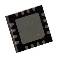
Need more?
| Packaging Type | Quantity | Unit Price: | Total |
|---|---|---|---|
| Cut Tape | 1 | CNY127.500 | CNY127.50 |
| Quantity | Price (inc GST) |
|---|---|
| 1+ | CNY127.500 (CNY144.075) |
| 10+ | CNY100.650 (CNY113.7345) |
| 25+ | CNY93.910 (CNY106.1183) |
| 50+ | CNY90.240 (CNY101.9712) |
| 100+ | CNY86.570 (CNY97.8241) |
| 250+ | CNY85.700 (CNY96.841) |
Product Information
- ManufacturerONSEMIManufacturer Part NoNB6N14SMNR2GCopyManufacturer Standard Lead Time44 weeksOrder CodeRe-Reel3368250RLCut Tape3368250Technical DatasheetClock IC TypeFanout Buffer, TranslatorClock Buffer TypeFanout Buffer, TranslatorFrequency2GHzClock IC Case StyleQFNNo. of Outputs4OutputsSupply Voltage Min3VSupply Voltage Max3.6VIC Case / PackageQFNNo. of Pins16PinsProduct Range-Qualification-Operating Temperature Min-40°COperating Temperature Max85°CSVHCNo SVHC (25-Jun-2025)
Product Overview
NB6N14SMNR2G is a differential 1:4 clock or data receiver and will accept AnyLevel differential input signals: LVPECL, CML or LVDS. These signals will be translated to LVDS and four identical copies of clock or data will be distributed, operating up to 2.0GHz or 2.5Gb/s, respectively. As such, the NB6N14S is ideal for SONET, GigE, fibre channel, backplane and other clock or data distribution applications. The NB6N14S has a wide input common mode range from GND + 50mV to VCC - 50mV. Combined with the 50 internal termination resistors at the inputs, the NB6N14S is ideal for translating a variety of differential or single−ended Clock or Data signals to 350mV typical LVDS output levels.
- Maximum input clock frequency <gt/> 2.0GHz
- Maximum input data rate <gt/> 2.5Gb/s
- 1ps maximum RMS clock jitter
- Typically 10ps data dependent jitter
- 380ps typical propagation delay
- 120ps typical rise and fall times
- VREF_AC reference output
- TIA/EIA − 644 compliant
- Functionally compatible with existing 3.3V LVEL, LVEP, EP and SG devices
Technical Specifications
- Clock IC Type
Fanout Buffer, Translator
Frequency2GHz
No. of Outputs4Outputs
Supply Voltage Max3.6V
No. of Pins16Pins
Qualification-
Operating Temperature Max85°C
SVHCNo SVHC (25-Jun-2025)
Clock Buffer TypeFanout Buffer, Translator
Clock IC Case StyleQFN
Supply Voltage Min3V
IC Case / PackageQFN
Product Range-
Operating Temperature Min-40°C
MSLMSL 1 - Unlimited
Technical Docs 1
Legislation and Environmental
- Country of Origin:
Country in which last significant manufacturing process was carried outCountry of Origin:Thailand
Country in which last significant manufacturing process was carried outTariff No:85423990US ECCN:EAR99EU ECCN:NLRRoHS Compliant:YesRoHS
RoHS Phthalates Compliant:YesRoHS
SVHC:No SVHC (25-Jun-2025)Download Product Compliance CertificateProduct Compliance Certificate
Weight (kg):.000117