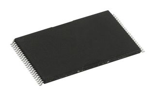
MT29F2G16ABAEAWP-AIT:E
闪存, SLC NAND, 2 Gbit, 128M x 16位, 并行口, TSOP-I, 48 引脚

需要更多?
| 数量 | 价钱 (含税) |
|---|---|
| 1+ | CNY233.940 (CNY264.3522) |
产品概述
MT29F2G16ABAEAWP-AIT:E is a NAND flash device which includes an asynchronous data interface for high-performance I/O operations. This device uses a highly multiplexed 8-bit bus (I/Ox) to transfer commands, address, and data. There are five control signals used to implement the asynchronous data interface: CE#, CLE, ALE, WE#, and RE#. Additional signals control hardware write protection and monitor device status (R/B#). This hardware interface creates a low pin-count device with a standard pinout that remains the same from one density to another, enabling future upgrades to higher densities with no board redesign. A target is the unit of memory accessed by a chip enable signal. A target contains one or more NAND flash die. A NAND flash die is the minimum unit that can independently execute commands and report status. A NAND flash die, in the ONFI specification, is referred to as a logical unit (LUN).
- 2Gb density, 16-bit device width
- 3.3V (2.7 to 3.6V) operating voltage
- Feature set E, Async interface
- Single-level cell (SLC) technology, command set: ONFI NAND flash protocol
- Operation completion, pass/fail condition, write-protect status
- Program page cache mode, read page cache mode, one-time programmable (OTP) mode
- Ready/busy# (R/B#) signal provides a hardware method of detecting operation completion
- WP# signal: write protect entire device
- Automotive industrial temperature from -40°C to +85°C
- Package style is 48-pin TSOP
技术规格
- 闪存类型
SLC NAND
记忆配置128M x 16位
IC 外壳 / 封装TSOP-I
时钟频率最大值50MHz
电源电压最小值2.7V
额定电源电压3.3V
工作温度最小值-40°C
产品范围2.7V-3.6V SLC NAND Flash Memories
存储密度2Gbit
接口并行口
针脚数48引脚
存取时间16ns
电源电压最大值3.6V
芯片安装表面安装
工作温度最高值85°C
法律与环境
- 原产地:
进行最后一道重要生产流程所在的地区原产地:Singapore
进行最后一道重要生产流程所在的地区税则号:85423275US ECCN:3A991.b.1.aEU ECCN:NLRRoHS 合规:是RoHS
RoHS 邻苯二甲酸盐合规:是RoHS
下载产品合规证书产品合规证书
重量(千克):.000001